
【Application Case】Spectral Confocal Scanning Measurement of Wafer Topography
Nov 12, 2024
Abstract: This application case involves the use of TronSight spectral confocal displacement sensors for scanning and measuring the topography of wafers. In the semiconductor manufacturing process, the topography of wafers plays a crucial role in the performance and reliability of chips. By measuring the wafer topography, parameters such as surface roughness, flatness, and thickness can be monitored in real-time throughout various manufacturing stages, ensuring that the wafers meet quality standards.
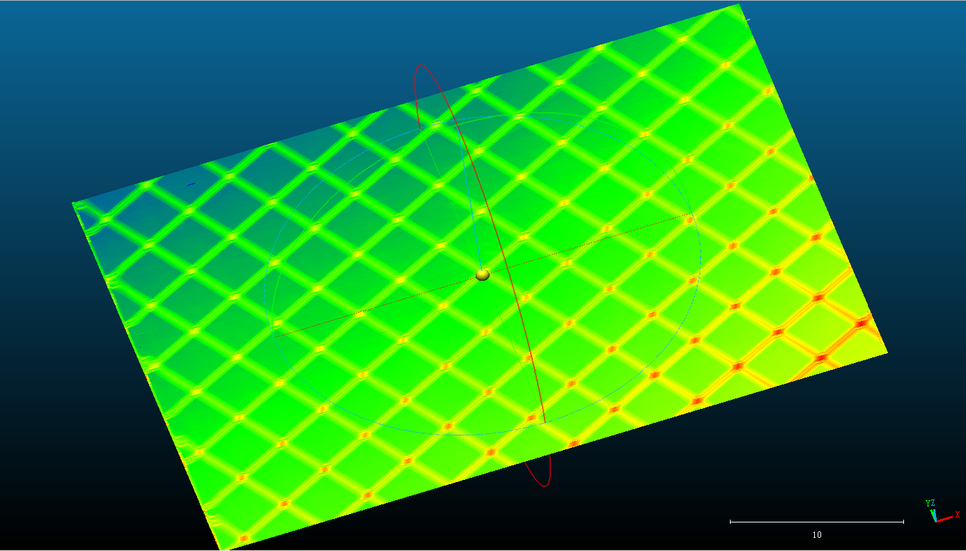
1.Wafer Topography Scanning Measurement Method:
(1)Preparation before scanning: Prepare a wafer, a three-dimensional motion platform, and a TS-400 probe with controller.
(2)Connection and fixation: Connect the probe to the controller and fix the probe on the three-dimensional motion platform. Then place the wafer under the probe.
(3)Distance adjustment: Adjust the distance between the probe and the wafer surface to ensure it is at the center of the probe's measurement range. Next, open the upper computer software and configure the sensor parameters.
(4)Platform parameter setting: Configure the parameters of the three-dimensional motion platform to ensure that the probe's light spot remains on the surface of the wafer during scanning.
(5)Start scanning and recording data: Initiate the scanning program and record the relevant data.
(6)Data analysis: Conduct in-depth analysis of the recorded data.
2.Scan Video


Recent Posts


Contact US
Product Information
Quantity
Unit
Piece
Support order samples, customization, wholesale direct, and complete payment. If the product you look for does not have corresponding customized content, pls fill out the form below to contact us, and we will reply ASAP.