
Wafer Flatness Measurement in Semiconductor Manufacturing
Sep 09, 2025
In semiconductor manufacturing, precision isn’t optional—it’s the rule of the game. One factor that has a huge impact on chip yield and reliability is wafer flatness—in simple terms, how smooth and even the wafer surface is. Even nanometer-level deviations can throw off critical processes like lithography, bonding, or thin-film deposition.
Why Wafer Flatness Matters
A wafer that isn’t flat can cause overlay errors during photolithography, misalignment during packaging, or uneven film thickness during deposition. According to SEMI M1 standards, flatness is defined as the deviation of the wafer surface from an ideal reference plane (SEMI, 2018).
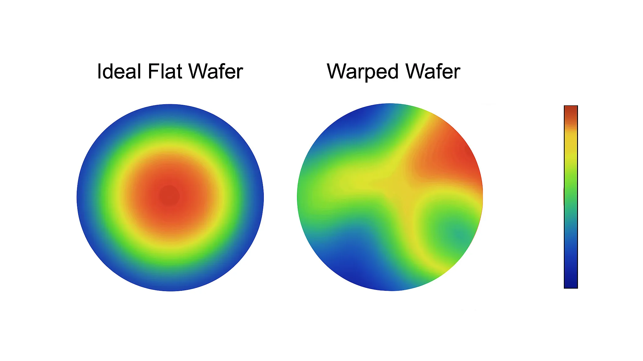
Studies confirm how important this is. Research from SPIE highlights that at sub-10 nm nodes, wafer planarity directly affects critical dimension (CD) uniformity and yield (Huang et al., 2017).
How Flatness Is Measured
Different technologies are used to measure wafer flatness, each with its own strengths:
-
Optical Interferometry – Captures interference fringes to detect surface variations with nanometer accuracy (Suzuki et al., 2003).
-
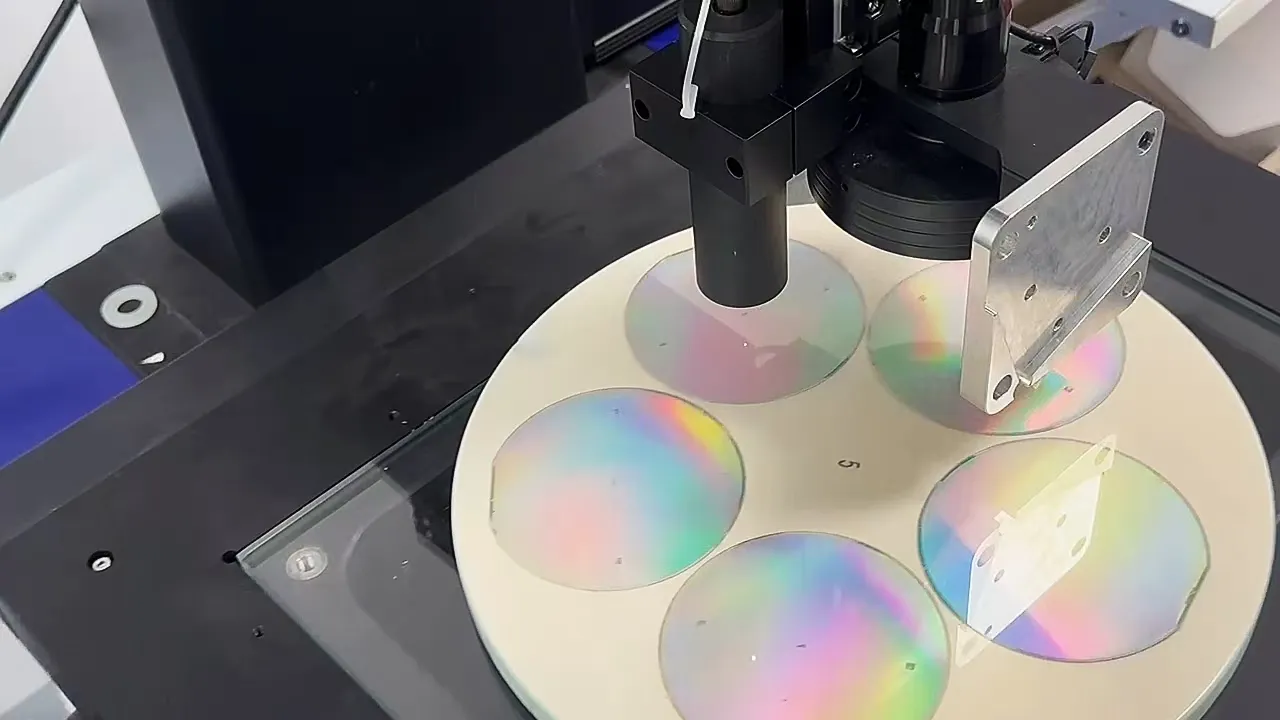
Chromatic Confocal Sensors – Offer fast, high-precision scanning without touching the wafer. TronSight’s TS-C series is a great example, providing sub-micron accuracy and high-speed sampling.
-
Infrared & White Light Interferometry – Best for transparent or multilayer wafers.
| Method | Contact / Non-Contact | Accuracy | Throughput | Advantages | Limitations | Typical Use Case |
|---|---|---|---|---|---|---|
| Contact Profilometry | Contact | High (nm level) | Low | Simple principle, proven accuracy | Risk of wafer damage, slow measurement speed | R&D labs, small wafer sampling |
| Laser / White Light Interferometry | Non-contact | Very High (sub-nm) | Medium | Extremely high precision, well established | Sensitive to vibration, dust, expensive | Advanced fabs, metrology labs |
| Chromatic Confocal Sensors | Non-contact | High (sub-μm) | High | Fast, stable, flexible for inline systems | Needs calibration for larger wafer diameters | Inline wafer mapping, inspection |
The right choice depends on wafer material, transparency, and resolution needs.
Industry Standards and Guidelines
Flatness isn’t just a matter of preference—it’s standardized so fabs worldwide can align on quality. The SEMI standards are the most widely followed references:
-
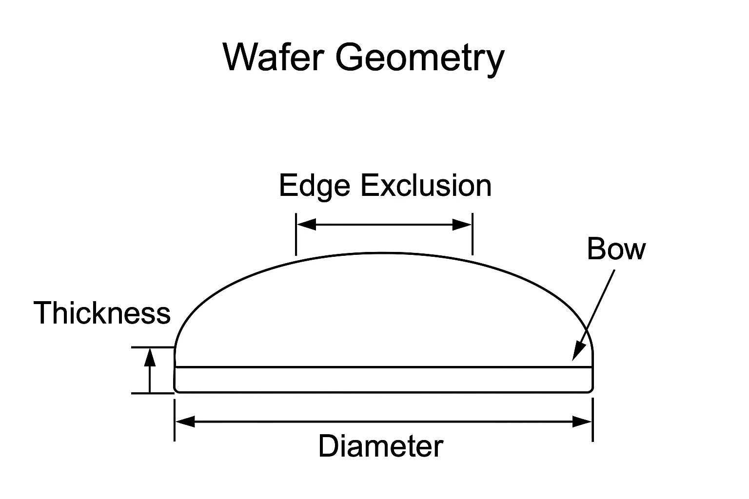
SEMI M1: Defines wafer flatness metrics like TTV (Total Thickness Variation), Bow, and Warp.
-
SEMI M62: Outlines how to measure and present wafer geometry data.
Applications in Semiconductor Processes
Flat wafers are critical in multiple steps across the semiconductor value chain:
-
Lithography: Focus and exposure accuracy depend on surface flatness.
-
Wafer Bonding: Non-flat wafers can cause weak bonding or air gaps.
-
Thin-Film Deposition: Uniform thickness requires a stable, even base.
Our solution & Conclusion
Wafer flatness might seem like a small detail, but in semiconductor manufacturing, small details make all the difference. By following SEMI standards and using advanced metrology tools like TronSight’s TS-C series, fabs can reduce variability, boost yield, and stay competitive in the era of nanometer-level manufacturing.
TS-C Series in Action
TronSight’s TS-C Series Chromatic Confocal Displacement Sensors are designed for high-precision, versatile displacement and surface measurements. Key features include:
-
Ultra-High Sampling Speed: Supports up to 32 kHz sampling, ensuring fast and accurate data acquisition.
-
Multi-Channel Synchronous Sampling: Up to 16 channels can sample simultaneously, allowing multiple points to be measured at once for comprehensive surface analysis.
-
Small, Flexible Probe Design: Probe outer diameter as small as φ3.8 mm with a maximum measurement angle of +60°, making it compatible with tight spaces and complex geometries.
-
Environment Compatibility: Operates reliably in high-temperature or vacuum conditions, supporting challenging lab or industrial environments.
-
Multi-Layer Measurement Capability: Can measure through multi-layer glass, enabling applications in optics, electronics, and material research.
-
Industrial Connectivity: Fully compatible with EtherCAT bus protocol for integration into automated systems, facilitating real-time data transfer and analysis.
These specifications make the TS-C Series a versatile tool for precise displacement, thickness, and surface profiling tasks, providing micron-level resolution and robust performance across a variety of conditions.
References
-
SEMI M1-2018, Specifications for Polished Single Crystal Silicon Wafers. SEMI International Standards.
-
SEMI M62-1110, Guide for Presentation of Wafer Geometry Data. SEMI International Standards.
-
Huang, R. et al. (2017). Wafer geometry control for advanced lithography. SPIE Journal of Micro/Nanolithography.
-
Suzuki, M. et al. (2003). Interferometric techniques for wafer flatness measurement. IEEE Transactions on Semiconductor Manufacturing.


Recent Posts

October 26, 2016
The Most Successful Engineering Contractor


Contact US
Product Information
Quantity
Unit
Piece
Support order samples, customization, wholesale direct, and complete payment. If the product you look for does not have corresponding customized content, pls fill out the form below to contact us, and we will reply ASAP.