
SEMI03.Wafer Two-sided Geometric Topography Measurement
Jul 30, 2025
Wafer Two-sided Geometric Topography Measurement
Application Overview
In semiconductor manufacturing, double-sided wafer processes—especially involving Si, SiC, and GaN wafers—are critical to high-performance chip design. Understanding the geometric topography on both front and back surfaces is essential for ensuring die flatness, minimizing warpage, and improving wafer bonding accuracy during packaging or advanced lithography. Typical measurement targets include bow, warp, TTV (total thickness variation), surface roughness, and parallelism between both sides.
TronSight's laser displacement sensors and chromatic confocal sensors provide high-precision, non-contact solutions for simultaneous double-sided topographic profiling, even under high throughput requirements.
Measurement Process
-
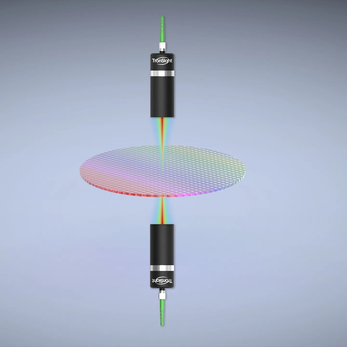
Sensor Configuration:
A pair of high-resolution displacement sensors are mounted face-to-face, aligned precisely to scan the front and back wafer surfaces in parallel. Common system configurations use two TS-P series laser triangulation sensors or TS-C chromatic confocal probes. -
Wafer Handling:
The wafer is positioned on a vacuum chuck or robotic arm, often held at the edge to avoid surface contamination or damage. -
Full-surface Scanning:
As the wafer is moved linearly or rotated on a stage, the sensors simultaneously capture Z-axis data from both sides at high frequency. -
Data Synchronization & Processing:
Dual-sensor data is synchronized and analyzed in software to extract key metrics such as front-back surface profiles, total thickness variation, and differential warpage.
Why It Matters
Double-sided wafer topography has become a key quality metric in 3D packaging, MEMS device fabrication, and wafer-to-wafer bonding processes. Excessive warp or TTV may lead to alignment failure, void formation, or yield loss during chip stacking or bonding.
Accurate profiling of both wafer surfaces enables:
-
Inline warpage control: real-time feedback for CMP, grinding, or thinning steps.
-
Improved packaging reliability: especially in TSV or fan-out processes.
-
Minimized bonding defects: critical for Si/SiC wafer bonding in power electronics.
-
Optimized process parameters: through feedback into polishing or cleaning steps.
Compared with stylus or contact systems, TronSight's optical non-contact solution ensures micron-level resolution without surface damage, making it suitable for both R&D and mass production lines.
Tronsight's Recommended Product Configurations
-
TS-C Series (Chromatic Confocal Displacement Sensor)
– Axial Resolution: down to 5 nm
– Suitable for transparent, mirror, and rough surfaces.
– Offers superior precision for R&D and hybrid metrology stations.
Recommanded model: TS-C7000←click for more details
For double-sided setups, both sensors can be integrated into a single measurement module with precision alignment jigs and software-controlled synchronization.
Contact our application engineer:
Send a message: Contact us
Email: service@tronsight.com


Recent Posts

October 26, 2016
The Most Successful Engineering Contractor


Contact US
Product Information
Quantity
Unit
Piece
Support order samples, customization, wholesale direct, and complete payment. If the product you look for does not have corresponding customized content, pls fill out the form below to contact us, and we will reply ASAP.