
SEMI04.Wafer Stage Parallelism Measurement
Jul 30, 2025
Wafer Stage Parallelism Measurement
Why It Matters
In semiconductor manufacturing, the wafer stage must move with high stability and precise alignment across all axes. Even the slightest misalignment or tilt of the wafer stage can lead to uneven exposure, incorrect lithography patterns, and ultimately, yield loss. Accurate parallelism measurement of the wafer stage ensures optimal alignment between the wafer surface and the optical axis or measurement plane. This is critical for front-end processes such as lithography, etching, and deposition, where sub-micron control determines the success of the final device. Implementing real-time, high-resolution measurement of wafer stage parallelism plays a crucial role in equipment calibration, process optimization, and overall production reliability.
Common Measurement Methods
| Method | Principle | Accuracy | Real-Time Capable | Non-Contact | Cost Level | Application Note |
|---|---|---|---|---|---|---|
| Laser Displacement Sensor (x2) | Measures Z-distance at two points, computes relative tilt | ±0.1 μm typical | ✅ | ✅ | Medium | Simple, stable for horizontal stage |
| Autocollimator | Detects angular deviations in reflection | ±0.5 arcsec | ❌ | ✅ | Medium-High | Requires mirror attachment |
| Interferometer | Uses optical interference to determine surface deviation | ±0.01 μm | ✅ | ✅ | High | High precision, complex setup |
| Capacitive Sensor | Measures capacitance variation to infer distance | ±0.05 μm | ✅ | ❌ | Medium | Sensitive to environmental factors |
Measurement Principle and Procedure
Using a pair of high-precision laser triangulation displacement sensors (e.g., Tronsight TS-P30), two Z-axis positions are measured simultaneously at different points on the wafer stage. By calculating the height difference and dividing it by the distance between the points, the angle of inclination (θ) is derived:
θ = arctangent(ΔZ / ΔL)
This method allows for real-time monitoring during stage movement or leveling adjustments. The sensors can be mounted facing down or horizontally, depending on the machine architecture. The data is streamed via high-speed interfaces for closed-loop control or logging.
Key benefits of this setup include:
-
Submicron resolution (0.02 μm)
-
Non-contact, non-destructive to wafer or chuck
-
High sampling rate (up to 160 kHz)
-
Compact and easy integration
Tronsight’s Solution
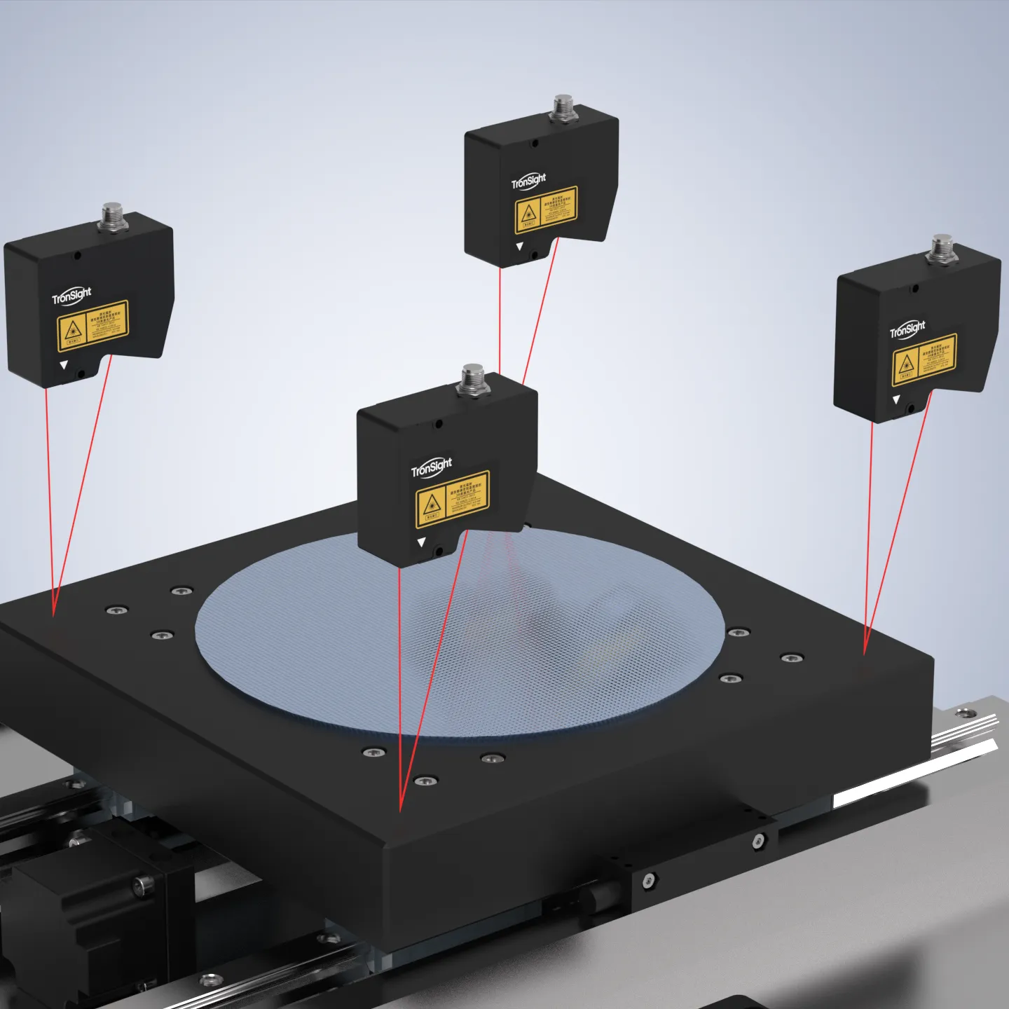
Tronsight provides a simple yet highly precise solution using dual TS-P30 laser triangulation displacement sensors. With its high sampling rate and ±0.02% F.S. linear accuracy, the TS-P30 ensures that even micro-level tilts or unevenness in the wafer stage are instantly detected and quantified. The system can be customized with fixtures to suit vacuum chucks or standard platforms.
Optional integration with the TS-CC controller enables multi-channel data acquisition, advanced filtering, and real-time visualization via Tronsight’s SDK. Whether for inline inspection or stage calibration, our solution ensures consistent measurement performance and fast deployment.
Product Recommendation & Contact
Recommended Sensor: TS-P150 Series←Click for more details
-
Measurement Range: 150±40mm
-
Sampling Rate: Up to 160 kHz
-
Repeatability: 1.2 μm
-
Ideal for high-speed motion platforms and wafer-level stage testing
Need a tailored measurement setup?
📞 Contact us on WhatsApp
📧 Or email: service@tronsight.com
We offer application guidance, fixture design suggestions, and remote technical support worldwide.


Recent Posts

October 26, 2016
The Most Successful Engineering Contractor


Contact US
Product Information
Quantity
Unit
Piece
Support order samples, customization, wholesale direct, and complete payment. If the product you look for does not have corresponding customized content, pls fill out the form below to contact us, and we will reply ASAP.